

Multilayer PCB
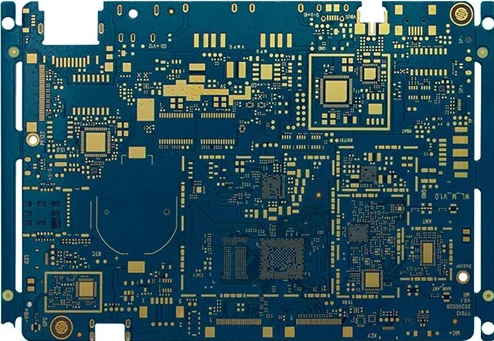
Multilayer PCB is a circuit board that has more than two layers. Unlike a Double-Sided PCB which only has two conductive layers of material, all multilayer PCBs must have at least three layers of conductive material which are buried in the center of the material.
More Information
|
Multilayer PCB Production Capability |
|
|
Item |
Capability |
|
Layer Count |
1-40layers |
|
Base Material |
KB、Shengyi、ShengyiSF305、FR408、FR408HR、IS410、FR406、GETEK、370HR、IT180A、Rogers4350B、Rogers4000、PTFE Laminates(Rogers series、Taconic series、Arlon series、Nelco series)、Rogers/Taconic/Arlon/Nelco laminate with FR-4 material(including partial Ro4350B hybrid laminating with FR-4) |
|
Board Type |
Backplane、HDI、High multi-layer 、blind&buried PCB、Embedded Capacitance、Embedded resistance board 、Heavy copper power PCB、Backdrill. |
|
Board Thickness |
0.2-5.0mm |
|
Copper Thickness |
Min. 1/2 OZ, Max. 10 OZ |
|
PTH Wall |
25um(1mil) |
|
Maximum Board Size |
1100*500mm(43”*19”) |
|
Min laser drilling size |
4mil |
|
Min. Spacing/Tracing |
2.7mil/2.7mil |
|
Solder Mask |
Green, Black, Blue, Red, White, Yellow, Purple matte/glossy |
|
Surface Treatment |
Flash gold(electroplated gold)、ENIG、Hard gold、Flash gold、HASL Lead-free 、OSP、ENEPIG、Soft gold、Immersion silver、Immersion Tin、ENIG+OSP, ENIG+Gold finger, Flash gold(electroplated gold)+Gold finger, Immersion silver+Gold finger, Immersion Tin+Gold finger. |
|
Min. Annular Ring |
3mil |
|
Aspect ratio |
10:1(HASL Lead-free 、HASL Lead、ENIG、Immersion Tin、Immersion silver、ENEPIG);8:1(OSP) |
|
Impedance control |
±5ohm(<50ohm), ±10%(≥50ohm) |
|
Other Techniques |
Blind/Buried Via |
|
Gold Fingers |
|
|
Press Fit |
|
|
Via in Pad |
|
|
Electrical Test |
|